Advanced Packaging Market to Grow 8% to 2026
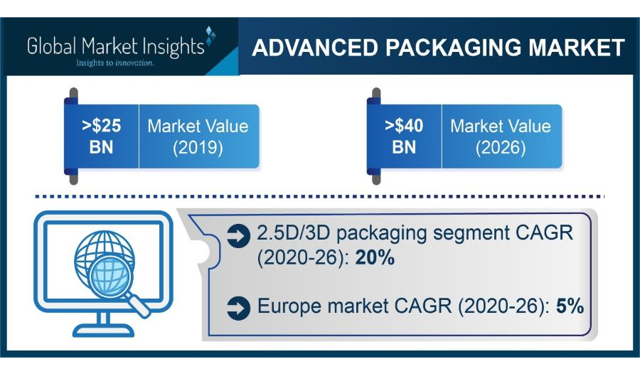
According to a recent study from market research firm Global Market Insights, the advanced packaging market is set to grow from its current market value of more than $25 billion to over $40 billion by 2026, gaining remarkable traction over the 2020 to 2026 period.
The advanced packaging market is poised to accumulate noteworthy gains in coming years owing to high product adoption across numerous application avenues such as healthcare, automotive, consumer electronics, aerospace & defense among others. Advanced packaging was developed to improve the performance of device and simultaneously shrink the packages. It is termed as a general grouping of a variety of different techniques such as system-in-package, 3D-IC, 2.5D, and fan-out wafer-level packaging.
Systems and appliances in several domains such as transportation systems, industrial, home appliances, medical, information among many others comprise of semiconductor chips. In fact, the process of semiconductor packaging is one of the most emerging sectors. Semiconductor packaging materials are known to be a class of electronic solutions utilized to form the connection of IC chip to the packaging substrate.
Advanced packaging market is bifurcated in terms of packaging type, application, and regional landscape.
With respect to packaging type, the advanced packaging market is classified into 2.5D/3D, fan-out, embedded-die, fan-in WLP, and flip-chip. Among these, fan-in WLP segment will witness considerable growth over the coming years. In 2019, the segment held a market share of over 10%. The growth is ascribed to the growing adoption of fan-in WLP by smartphone manufacturers to achieve high density and low form factor chipsets.
Fan-in wafer-level package is referred to the technology of packaging an IC (integrated circuit) at the wafer level. This technology is an extension of the wafer fab process and generally utilizes the conventional fab tools and processes. Wafer level package is an efficient batch process which packages almost each device on wafer concurrently. The FI-WLP is considered a true CSP (chip-scale package) technology, since the resulting package is of the same size as the die.
In terms of application, the overall advanced packaging market is segmented into aerospace & defense, healthcare, industrial, automotive, consumer electronics and more. Among these, the healthcare application segment is slated to witness remarkable growth over the coming years. In 2019, the segment accounted for around 5% industry share.
The growth is attributed to the growing adoption of AI chipsets across healthcare applications mainly for remote monitoring, which is further likely to increase the demand for advanced packaging. In addition, the growing need for advanced packaging for miniaturized devices is also driving the product demand across healthcare application.